


PCB and PCB wet process
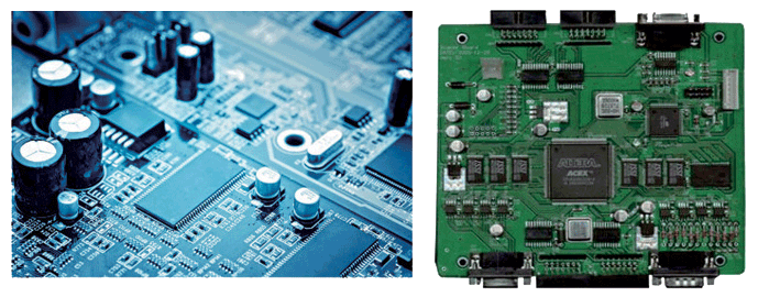
In the electronics industry, circuit boards are the basic carrier for the connection of electronic components. On an insulated substrate, the copper plate is etched into an engineering circuit. Because of the screen printing method, it is called a printed circuit board (PCB).After installing electronic components on the board, a printed circuit assembly (PCA) is formed.Because PCB is cheap and very durable, and can be continuously produced in large quantities, it is used in almost all fields of electronic devices.
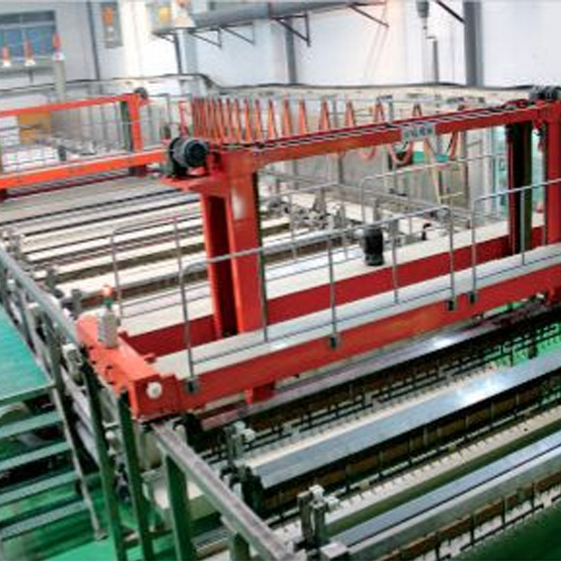
The electroplating technology research and Development center established by Kunshan Dongwei specializes in electroplating technology in the PCB industry, and continuously introduces processes and equipment that meet the requirements of new products to provide customers with unique special equipment.These equipment cover PCB primary copper, secondary copper, PTH flow, nickel-gold and other processes.
Traditional PCBs have actual product functional requirements and are divided into single-panel, double-panel, multi-layer, and flexible boards.
With the rapid development of technology, IC carrier boards and roll-to-roll flexible boards have also appeared.No matter what form of PCB it is, in the traditional manufacturing process, thin lines, multiple layers, and ultra-thin surfaces increasingly challenge the process capabilities of PCB manufacturers.Among them, the wet process, especially the electroplating link, is the key factor in the entire PCB production.

Desmear+PTH process
Feeding → leavening → washing → potassium permanganate → recovery → hot water washing → washing → degreasing → hot water washing → washing → micro-etching → prepreg → activation → washing → quickening → washing → chemical copper → washing → cutting
Primary copper process
Feeding → cleaning → washing → micro-etching → washing → prepreg → electroplating copper → washing → cutting → stripping → washing
Secondary copper process
Feeding → cleaning → washing → micro-etching → washing → prepreg → electroplating copper → washing → prepreg → electroplating tin → washing → cutting → stripping → washing
Nickel plating process
Feeding → cleaning → washing → micro-etching → washing → pickling → washing → nickel plating → washing → activation → washing → gold plating → recycling → washing → cutting


Project Manager WeChat

Mobile version official website